
BOM estimated cost: ¥ 13.50 PCBA estimated cost: ¥ 10.50 Estimated cost of finished product: ¥ 14.80
An Introduction
The general advantages of the program are as follows:
1. Compatibility: almost all mobile phone fast charging protocols are supported, and QC2.0 / 3.0, PE1.0, AFC, FCP, SCP, VOOC, BC1.2 DCP, APPLE 2.4A fast charging protocols are integrated inside.
2. Low temperature: At a room temperature of 25 ° C, the surface temperature of the MOS and inductor is up to 67 ° C, and the temperature of the finished case is only 38 ° C.
3. Safety: fast charge when any one port is inserted, and the output voltage drops to 5v when both ports are inserted at the same time to exit the fast charge, which plays a protective role; a solid capacitor is 10 times more expensive and there is no risk of explosion; the chip voltage value can be It reaches 40v; the chip integrates multiple safety protection functions such as output undervoltage, short circuit protection, overcurrent protection and so on.
4. Application range: wide range, 12v ~ 35v car and truck can be used, excluding vehicles with abnormal voltage higher than 35v.
5. The mass production price is lower, and the profit margin is large: the dual usb port is completed by one chip, reducing costs
6. Program reliability: high reliability, this program has undergone 7 times of optimization and modification and finally formed;
Supports over-voltage / under-voltage, over-current, short circuit and other protection functions, high safety, good reliability, simple production, is the most complete fast charging protocol on the market, the best compatibility is a cost-effective fast charging car charging solution.
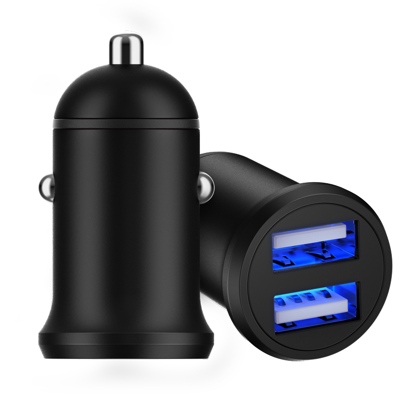
Application range
Car phone fast charging.
Features
Two-way fully compatible QC / PE / AFC / FCP / SCP / VOOC single-chip fast charging car charging solution.
Completed the DC-DC step-down and fast charge protocol with a single chip. The solution has high integration, few peripheral originals, and excellent thermal efficiency. The component temperature is below 70 ° C. Support BC1.2 DCP / QC / PE / AFC / FCP / SCP / VOOC, Apple 2.4A all mobile phone fast charging protocols. The output power is up to 24W, tested almost all fast charge protocol mobile phones on the market, the compatibility is almost 100%, supports over-voltage / under-voltage, over-current, short circuit and other protection functions. High safety, good reliability, simple production , Is the most complete fast charging protocol on the market, with the best compatibility and a cost-effective fast charging car charging solution.
Features
✔ Support BC1.2 DCP, QC2.0, QC3.0, PE1.0, AFC, FCP, SCP, VOOC, APPLE 2.4A fast charging protocol, compatible with almost all relevant mobile phones on the market.
✔ Two A-port outputs: Each channel supports fast charging.
✔ Output power up to 24W
✔ Discharge efficiency: greater than 93% @ 5V / 3A
✔ Adaptive output voltage
✔ Power on LED indication
✔ Fast charge LED indicator
✔ Insert any A port output to support fast charging. After both A are plugged into the mobile phone and exit the fast charging, the output voltage drops to 5V
✔ Overcurrent, overvoltage / undervoltage, short circuit protection
✔ Input voltage range: 8.0V ~ 28V (withstand voltage 40V)
✔ Output voltage range: 3.8V ~ 12V
✔ Chip withstand voltage 40V
Q & A:
Q1: Can the housing of the input / output interface be connected to GND?
A1: No. Because the negative electrode of some interface connection wires is connected to the shell, and our sampling resistor needs to be connected between GND and the negative electrode of the interface, if the two are connected, it is equivalent to a short circuit of the sampling resistor.
Q2: Does the product not support fast charging of mobile phones?
A2: The mobile phone is not compatible with fast charging, it may be because a suitable charging cable has not been purchased. If it is indeed incompatible, you can feedback to us.
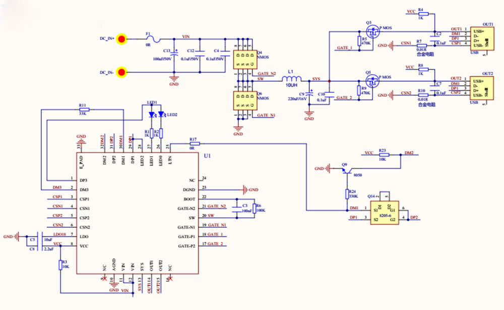
Application circuit diagram
PCB design reference:
1. Copper heat dissipation is required under the IC (the IC substrate should be connected to PGND), the heat dissipation area should be as large as possible, and the substrate pad is drilled through
The bottom layer of the PCB, and properly exposed copper to enhance heat dissipation.
2. The 10uF capacitor of the LDO18 pin should be close to the chip pin; AGND returns to PGND in a single point connection.
3. The sampling resistor CSP, CSN terminal layout should follow the following rules:
A) CSP, CSN wiring should try to avoid interference source devices such as inductors, loop MOS, Vout, etc .;
B) CSP, CSN wiring should be on the same layer as much as possible to reduce the situation of punching holes;
C) Both the CSP and CSN lines must be close to the sampling resistor, and the parallel wiring from the two ends of the sampling resistor to the chip and
As close as possible to the chip; the connection between the sampling resistor and the chip end must not be overcurrent. The same principle CSN is also not possible
Connect directly to PGND.
4. Large current path (part of the circuit of the buck-boost loop: BAT – inductance – MOS-VOUT): try to walk on the same layer,
And as thick and short as possible, at the same time the area of the ground should also be increased and complete. This can increase heat dissipation, reduce ripple and reduce
EMC interference.
5. The shell of the USB port cannot be directly connected to GND. Because some of the negative pole of the USB cable is connected to the shell, the sampling
Resistance needs to be connected between the negative terminal of the interface and GND. If the two are connected, it means that the sampling resistor is shorted.
6. In order to ensure the best performance of heat dissipation and EMC, it is recommended to use a four-layer board.
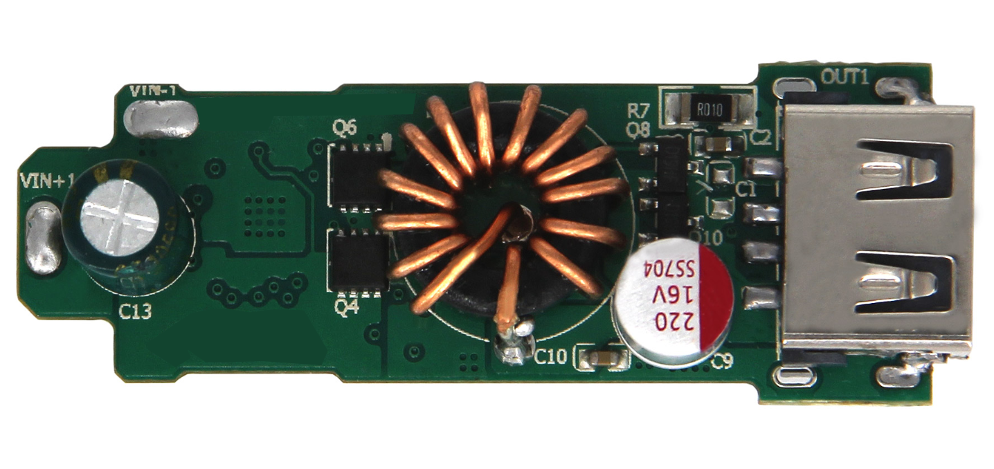
PCBA
Provide services
PCB customization: self-operated factory, can produce 1-34-layer high multilayer board and HDI board (1-2 steps, blind buried holes), support proofing and batch production; proofing plant production capacity of 20,000 square meters / month
SMT processing: 10 SMT production lines, equipped with imported high-end high-speed placement machines, supporting double-sided full placement, DIP plug-in welding, BGA and other special placement; can be used to open steel mesh, purchase materials, accept customer supply, professional management , One-stop solution
ODM: R & D and design of finished products to production and assembly services, and assembly of own finished products.

Scan the QR Code with WhatsApp
WeChat
Scan the QR Code with WeChat