Printed circuit boards (PCBs) with a copper foil thickness equal to or greater than 105 μm (≥3 oz) are referred to as thick copper printed circuit boards. The application field and demand for thick copper PCB have been rapidly expanded in recent years, and it has become a popular PCB variety with good market development prospects. Most of the thick copper printed circuit boards are high current substrates, and the large current substrates are mainly used in power supply modules (power modules) and automotive electronic components. The development trend of such a large current substrate is to carry a larger current, the heat generated by a larger device needs to be dissipated, and the thickness of the copper foil used for the substrate is also thicker and thicker. For example, the current production of high-current substrates using 210 μm thick copper foil has become conventional; for example, instead of the busbars used for automobiles, robots, power supplies, etc., the thickness of the conductor layer of the substrate has reached 400 μm. ~2000 μm.
Thick copper printed circuit boards above 105 μm have difficulties in solder mask fabrication. Due to the limitation of the thickness of the ink on the substrate (the requirement of the ink mark on the substrate and the excessive thickness of the ink on the substrate may cause the problem of the substrate position soldering crack after the printed circuit board is soldered), the electrostatic spraying or spraying process cannot be used. produce. At present, the two processes in the industry can only use traditional screen printing: one is to print multiple solder masks, the other is to make the substrate first, and the substrate is filled with solder mask and used as a normal PCB normal solder resist. However, screen printing will cause quality problems such as solder-welding holes, broken soldering bridges, and air bubbles between lines. How to achieve it can be produced using an electrostatic spray or spray process. And to ensure that the substrate position soldering thickness is not too thick? This is the purpose of our research.
1 Method implementation
1.1 Planning stage
(1) Planning direction. The method provided is to change the design engineering data to make a solder mask exposure film to achieve. The ink on the substrate position after the previous multiple soldering is developed and the ink on the line side is retained. The last time it is normally produced as a conventional PCB, so that there is only one solder mask on the substrate, and there is no problem that the line is red.
(2) Planning process. Pre-weld treatment → plug hole → electrostatic spray → alignment exposure (special design film) → development → post-weld soldering → pre-weld treatment → plug hole → electrostatic spray → alignment exposure 1 (normal film) → development → resistance Post-weld bake 1...
2.2 Test phase
(1) Multiple solder masks were produced in the front. It is produced by electrostatic spraying or spraying process (to avoid soldering into the hole during spraying), and is produced by solder mask exposure using specially designed solder mask exposure film data.
(2) The last solder mask production. It is produced by electrostatic spraying or spraying process (to avoid soldering into the hole during spraying), and the normal solder mask is used to expose the film data during solder mask exposure. The effect after solder mask finish is shown in Figure 1.
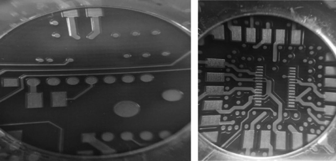
Figure 1 Effect after completion of solder mask
(3) substrate position ink thickness section (Figure 2)
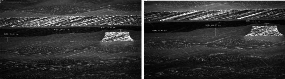
Figure 2: Solder mask cutaway
2.3 Standardization and promotion stage
The production board is subjected to small-volume and medium-batch tests using the materials and processes designed and developed by the process, and the batch test results are consistent with the test results in the initial stage of the test. For all copper thick printed circuit boards with a thickness of more than 105 mm, if this process is used in the production of solder mask, the quality of the product can be greatly improved.
3 results
On the one hand, the development of the above new technology can be used to solve the problem of solder-resistance holes, broken-resistance solder bridges and wires that can not be solved by conventional screen printing in the case of solder-resistance of 105 mm thick copper printed circuit boards. Quality problems such as bubbles, while avoiding the problem of solder mask cracking caused by excessive soldering at the substrate position of the solder resist, allowing the 105 mm thick copper printed circuit board to be smoothly mass-produced and capable of satisfying customers at the same time. The quality requirements for solder mask.
After using the above process, the bottleneck of the smooth production of thick copper printed circuit boards of 105 mm or more is solved, and the scrap rate is reduced from 1.2% to 0.3%, so that a large number of thick copper printed circuit boards of 105 mm or more are used for power products. As well as communications, power, aerospace and other fields have been guaranteed.

Scan the QR Code with WhatsApp


WeChat
Scan the QR Code with WeChat